

High-Frequency Material · High-Speed Substrate Material
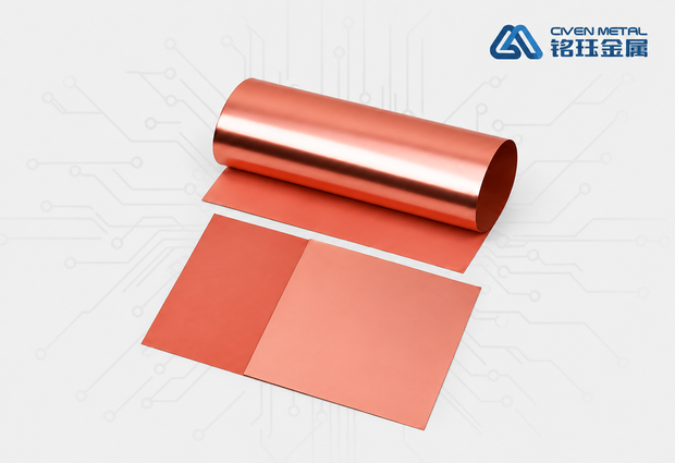
VLP Very Low Profile Electrodeposited Copper Foil
A key base material for 5G communications, AI servers and high-frequency, high-speed PCBs. Its very low surface roughness significantly reduces signal transmission loss and meets the demands of high-density interconnect (HDI) and fine-line manufacturing.
Contact Us >>What is VLP
What Is VLP Very Low Profile Copper Foil?
VLP (Very Low Profile) refers to Very low profile or ultra-low profile copper foil, a core category in the low-profile electrodeposited copper foil family. It is produced by precision electrodeposition: a high current density is applied in a copper sulfate plating solution to deposit copper onto a high-speed rotating cathode drum. The finished foil has a smooth drum side and a matte side, both with very low surface roughness (Rz ≤ 2 μm), and its grains are fine and equiaxed rather than conventionally columnar.
Compared with standard electrodeposited foil (STD) and low profile foil (LP), VLP foil has a significantly lower surface profile. This property directly addresses the core challenge of high-frequency, high-speed circuits: at high frequencies, the skin effect causes current to travel mainly along the conductor surface, so the rougher the surface, the greater the signal loss (worsening insertion loss IL and dielectric loss Df). With an extremely flat surface, VLP minimizes signal transmission loss.
Key Process Characteristics
- Ultra-low roughness on both sides: both drum side and matte side reach Rz ≤ 2 μm
- Fine equiaxed grains: non-columnar structure with better isotropy
- High peel strength: strong bonding to high-frequency substrates such as PTFE and hydrocarbon resins
- Low alloy content: high purity with excellent conductivity and corrosion resistance
Surface Profile Comparison
Surface profile comparison
Technology roadmap: STD → LP (Low Profile) → VLP (Very Low Profile) → HVLP (Hyper Very Low Profile)
Applications
Main Uses & End Applications
VLP foil is combined with low-loss substrates to make high-frequency, high-speed copper clad laminates (CCL), widely used in high-end electronics with strict signal integrity requirements.
5G Communication Equipment
Core 5G infrastructure components such as base station antennas, RF front-end modules and mmWave devices, all requiring very low insertion loss.
AI Servers & Data Centers
High-performance GPU servers, AI accelerator cards, high-speed switches and routers. A single AI server can use up to ten times as much VLP/HVLP foil as a conventional server.
HDI Boards
Multilayer HDI boards and any-layer fine-line interconnects in smartphones, wearables and high-end consumer electronics.
Automotive Electronics
EV powertrain control boards, ADAS mmWave radar PCBs, in-vehicle high-speed networks and charging management systems.
Network Communication Equipment
High-frequency circuits in high-speed switch backplanes, optical communication modules, network connectors and test and measurement instruments.
Flexible Printed Circuits (FPC)
Foldable screens, flexible display modules, wearable flexible interconnects and other applications that require thin profiles and high bending reliability.
Specifications
Available Specifications
Standard and custom grades in multiple thicknesses, covering everything from conventional PCBs to extra-thick high-power boards.
| Model series | Nominal thickness | Areal weight | Surface roughness Rz | Peel strength | Typical applications |
|---|---|---|---|---|---|
| VLP-12E | 12 μm | ~107 g/m² | ≤ 2.0 μm | ≥ 0.8 kg/cm | HDI multilayer boards, FPC flexible boards |
| VLP-18E | 18 μm | ~161 g/m² | ≤ 2.0 μm | ≥ 0.9 kg/cm | High-frequency high-speed multilayer boards, smartphone mainboards |
| VLP-35E | 35 μm | ~305 g/m² | ≤ 2.0 μm | ≥ 1.0 kg/cm | 5G base stations, AI server mainboards (mainstream grade) |
| VLP-70E | 70 μm | ~610 g/m² | ≤ 2.5 μm | ≥ 1.0 kg/cm | High-power circuit boards, automotive electronics |
| VLP-105E | 105 μm | ~915 g/m² | ≤ 2.5 μm | ≥ 1.0 kg/cm | Heavy-copper power boards, defense and aerospace high-frequency boards |
| VLP-HF series | 12–70 μm | Custom | ≤ 1.8 μm | ≥ 1.0 kg/cm | Ultra-high-frequency (≥ 28 GHz) mmWave applications |
Supply Format
- Rolls: width up to 1295 mm
- Sheets: up to 1295 × 1295 mm
Quality Certifications
- IATF 16949 automotive quality management system
- ISO 9001 quality management system certification
- Compliant with IPC-4562 specification for electrodeposited copper foil
Why VLP
Product Advantages
Six core technical advantages, a complete material solution for high-frequency, high-speed PCB manufacturing.
Ultra-Low Signal Transmission Loss
The ultra-smooth Rz ≤ 2 μm surface greatly reduces conductor loss from the skin effect, with Df optimized to ≤ 0.002, ensuring high-speed signal integrity. Ideal for 5G mmWave and high-speed backplanes in AI servers.
Fine-Line Etching Capability
The fine equiaxed grain structure enables faster etching and more uniform side etching, supporting fine lines at L/S = 25/25 μm and below, with significantly fewer white spot defects and higher pattern resolution.
High Bonding Reliability
Achieves peel strength of ≥ 0.8–1.0 kg/cm while maintaining ultra-low roughness, with excellent bonding interfaces on low-loss substrates such as PTFE and hydrocarbon resins and no risk of copper powder transfer.
Precise Characteristic Impedance Control
Uniform thickness and a flat surface minimize signal propagation delay and keep characteristic impedance deviation within ±7%, meeting the strict impedance matching requirements of high-speed differential signals.
Higher Processing Yield
During lamination, the low-profile surface is less likely to pierce thin prepreg (PP) sheets, reducing short-circuit risk. It drills well and suits laser blind via processing, with no copper recrystallization after multiple laminations.
Wide-Temperature Stability
Maintains good mechanical strength and electrical performance at high temperatures (Tg ≥ 180°C), with excellent oxidation and corrosion resistance, extending PCB service life in harsh conditions.
VLP vs Conventional Copper Foil: Key Metrics Compared
| Metric | Standard foil (STD) | VLP very low profile | Improvement |
|---|---|---|---|
| Surface roughness Rz | 6–10 μm | ≤ 2 μm | ↓ 70–80% |
| Insertion loss @ 10 GHz | > 0.8 dB/in | ≤ 0.4 dB/in | ↓ ~50% |
| Minimum line width / spacing | ≥ 50/50 μm | ≥ 25/25 μm | 2× precision |
| Impedance deviation | ± 10% | ± 7% | ↑ Control precision |
Get VLP Copper Foil Samples & Technical Data
Our technical team can recommend the optimal thickness grade and matching substrate for your specific application.