

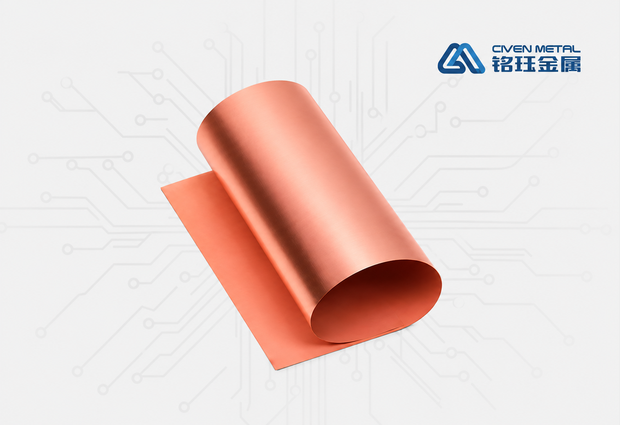
Reverse Treated Foil · Double-Side Treated Copper Foil
RTF Reverse Treated Double-Side Treated Copper Foil
Double-side treated copper foil with the shiny side of the electrodeposited foil also roughened. Both sides offer good bonding strength, eliminating the black-oxide step for multilayer inner layers. One of the mainstream choices for high-frequency, high-speed copper clad laminates.
· Product Features
- Rz 4–6 μm surface roughness
- Double-side roughened treatment
- No black oxide, streamlined process
- Df ≤ 0.015 Mid Loss grade
Roughness Evolution Roadmap
Surface Roughness Evolution
Product Introduction
Product Introduction
RTF (Reverse Treated Foil), also known as double-side treated copper foil, applies varying degrees of roughening to the drum side (shiny side) of conventional electrodeposited foil, which is normally smooth, so that both sides have good peel strength. Hence the name "reverse": the roughening treatment normally applied to only one side is "reversed" onto the other side.
The treatment level on each side is carefully designed: the side facing the dielectric is rougher (for stronger adhesion), while the roughened layer on the other side is thinner (preserving good etchability). This asymmetric double-side treatment meets two seemingly conflicting needs at once: strong bonding to the insulating substrate and easy etching during subsequent pattern transfer.
When used as inner-layer foil in multilayer boards, RTF's greatest practical value is eliminating the conventional black-oxide pre-treatment. The shiny inner-layer side of ordinary STD foil must be black-oxide treated before lamination to ensure bonding, while RTF has this step already done, directly shortening the process and lowering manufacturing costs. This is the core reason RTF has become the mainstream material for mid- to high-speed PCBs (1–10 Gbps).
Key Process Characteristics
- Double-side roughening: Both drum side and matte side are roughened to different degrees, giving both sides bonding strength
- Asymmetric treatment: Bonding side is rougher (strong adhesion), exposed side is thinner (easy etching)
- No black-oxide step: No additional oxidation treatment needed for inner layers; laminate directly
- Frequency range: 1–10 Gbps mid- to high-speed digital circuits
RTF double-side treatment structure
Specifications
Available Specifications & Parameters
Multiple thickness and roughness combinations to suit different layer stack-ups and cost budgets.
Supply Format
- Rolls: width up to 1295 mm
- Sheets: up to 1295 × 1295 mm
- Two roughness options: S / M
Core Value
- Eliminates inner-layer black-oxide (oxidation) pre-treatment
- Shortens multilayer board production cycle by 10–15%
- Lowers overall manufacturing cost
Applications
End-Use Applications
Serving every key sector of electronics manufacturing.
Servers & Storage
Rack server mainboard inner layers, storage array controller boards
Network Communications
Gigabit / 10-gigabit switch inner layers, router backplanes, firewall mainboards
HDI Multilayer Boards
Smartphone mainboards (8–12 layers), tablet mainboard inner layers
Automotive Electronics
In-vehicle infotainment systems, ADAS domain controller inner layers
5G Devices
5G phone / module mainboard inner layers, CPE devices
Consumer Electronics
High-performance laptop mainboards, game console mainboards
Core Advantages
Core Product Advantages
Building differentiated competitiveness.
Simplified Process
No black-oxide pre-treatment for inner layers; laminate directly and shorten production cycles
Balanced Bonding on Both Sides
Double-side roughening ensures sufficient adhesion whichever side faces the dielectric
Outstanding Cost-Effectiveness
20–40% cheaper than LP/VLP, meeting high-volume 1–10 Gbps demand
Good Etchability
The thin roughened layer on the exposed side makes clean fine lines easier to achieve than with STD
Mature Supply Chain
Ample global capacity, stable lead times and smaller price fluctuations than high-end series
Flexible Options
Two roughness levels (S/M) at the same thickness, selectable to match your actual loss budget
Get RTF Copper Foil Samples & Technical Data
Our technical team can recommend the optimal thickness grade and matching substrate for your specific application.