

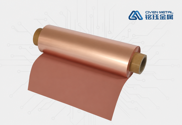
Hyper Very Low Profile Copper Foil
HVLP Hyper Very Low Profile Electrodeposited Copper Foil
The smoothest surface among today's commercial copper foils, with Rz as low as 1–1.5 μm. Designed for mmWave above 28 GHz and ultra-high-speed interconnects in AI training clusters, it is a foundational material for the computing era.
· Product Features
- Rz ≤ 1.5 μm lowest roughness
- Df < 0.003 Ultra Low Loss
- ≥ 56 Gbps ultra-high signal rate
- HVLP-1~5 sub-grades
Roughness Evolution Roadmap
Surface Roughness Evolution
Product Introduction
Product Introduction
HVLP (Hyper Very Low Profile) copper foil represents the highest level of today's commercial copper foil manufacturing. Building on VLP (Very Low Profile, Rz ≤ 2 μm), it pushes surface roughness further toward the physical limit, bringing Rz down to 1–1.5 μm or even lower (some HVLP-5 grades reach Rz ≤ 1.0 μm).
Why such an extremely smooth surface? The answer is the skin effect. At high frequencies (especially > 10 GHz), AC current does not flow evenly through the conductor cross-section but concentrates in a very thin "skin depth" layer at the surface; the higher the frequency, the shallower the skin depth. At 28 GHz mmWave, for example, the skin depth of copper is only about 0.4 μm. If the surface peaks and valleys (Rz) of the foil are much larger than the skin depth, current must "crawl" along a tortuous surface, greatly lengthening the effective path, sharply increasing resistance and severely attenuating the signal.
HVLP achieves a nearly atomically flat surface through tightly controlled electrodeposition parameters (ultra-low additive concentration, highly uniform current density and precise thermal field management). As a result, its insertion loss at 28 GHz and above is 60–70% lower than STD foil. As AI training clusters move to 56 Gbps / 112 Gbps SerDes rates and 5G-A / 6G mmWave commercialization accelerates, HVLP has become an irreplaceable strategic material.
Key Process Characteristics
- Surface roughness Rz: 1.0 – 1.5 μm (HVLP-5 reaches ≤ 1.0 μm)
- Sub-grades: Five grades: HVLP-1 / HVLP-2 / HVLP-3 / HVLP-4 / HVLP-5
- Typical Df: < 0.003 (Ultra Low Loss grade)
- Insertion loss @ 10 GHz: ≤ 0.35 dB/in, about 60% lower than STD
- Frequency range: ≥ 28 GHz mmWave / 56–112 Gbps high-speed SerDes
HVLP ultimate roughness comparison
Specifications
Available Specifications & Parameters
Five sub-grades covering the full high-speed spectrum from 25 Gbps to mmWave.
Supply Format
- Rolls: width up to 1295 mm
- Sheets: up to 1295 × 1295 mm
- HVLP-4/5 by advance order, lead time 4–6 weeks
Compatible Substrates
- PTFE (Ultra Low Loss grade)
- Hydrocarbon resin (Df < 0.003)
- Modified PPE/PPO, LCP liquid crystal polymer
Applications
End-Use Applications
Serving every key sector of electronics manufacturing.
AI Servers & Computing Clusters
GPU accelerator cards, TPU/NPU training boards, 56–112 Gbps SerDes high-speed interconnects
5G-A / 6G mmWave
28/39/77 GHz mmWave antenna modules, phased array radar transceiver units
Satellite Communications & Radar
Satellite-borne phased arrays, satellite internet ground stations, military electronic warfare systems
Ultra-High-Speed Switches
400GE / 800GE switch backplanes, co-packaged optics (CPO) substrates
Advanced Packaging
Redistribution layers (RDL) in 2.5D/3D IC packaging, conductive layers on glass substrates
Automotive mmWave
77 GHz mmWave radar PCBs, LiDAR control boards
Core Advantages
Core Product Advantages
Building differentiated competitiveness.
Industry's Lowest Roughness
Rz ≤ 1.5 μm (HVLP-5 reaches ≤ 1.0 μm), approaching the physical limit
Ultra-Low Signal Loss
Df < 0.003, with insertion loss 60%+ lower than STD
Supports 112 Gbps+
Meets the demanding requirements of next-generation AI computing and 6G mmWave
Five-Grade Selection
HVLP-1 to HVLP-5 precisely matched to different frequencies and cost budgets
Compatible with Top Substrates
Validated on ultra-low-loss substrates including PTFE, hydrocarbon resin and LCP
Strategically Scarce Resource
Global capacity is limited, and leading manufacturers have secured long-term supply
Get HVLP Copper Foil Samples & Technical Data
Our technical team can recommend the optimal thickness grade and matching substrate for your specific application.